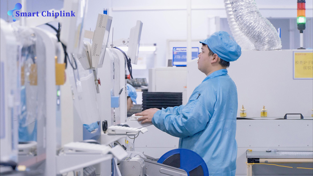
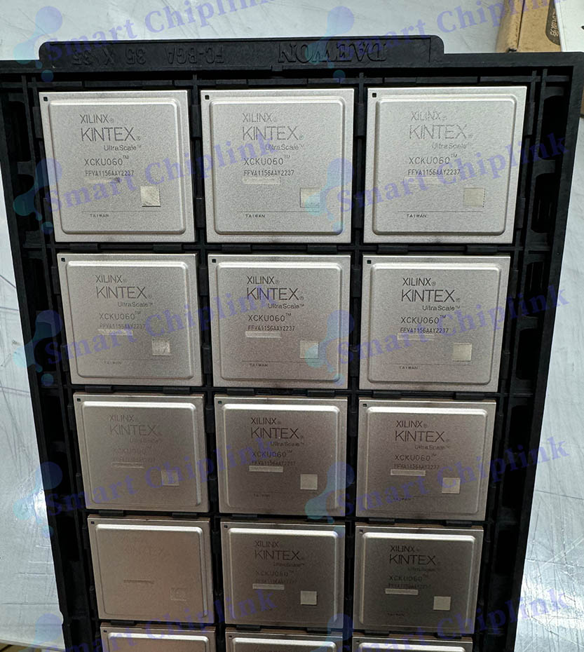
Today, 50PCS of Xilinx FPGA have been inspected.
We will arrange DHL international express to ship them to our client in Australia.
Part number is XCKU060-2FFVA1156E.
If you have any demand for original Xilinx FPGA, please feel free to click the ‘send inquiry’ button to contact us.
Feature
Processing System
UltraScale+ MPSoCs are built around a feature-rich quad-core ARM Cortex-A53 and dual-core ARM Cortex-R5 processing system (PS). In addition to the 32-bit/64-bit application processing unit (APU) and 32-bit real-time processing unit (RPU), the PS contains a dedicated ARM Mali™-400 MP2 graphics processing unit (GPU).
I/O, Transceiver, PCIe, 100G Ethernet, and 150G Interlaken
Data is transported on and off chip through a combination of the high-performance parallel SelectIO™ interface and high-speed serial transceiver connectivity. I/O blocks provide support for cutting-edge memory interface and network protocols through flexible I/O standard and voltage support. The serial transceivers in the UltraScale architecture-based devices transfer data up to 32.75Gb/s, enabling 25G+ backplane designs with dramatically lower power per bit than previous generation transceivers. All transceivers, except the PS-GTR, support the required data rates for PCIe Gen3, and Gen4 (rev 0.5), and integrated blocks for PCIe enable UltraScale devices to support up to Gen4 x8 and Gen3 x16 Endpoint and Root Port designs. Integrated blocks for 150Gb/s Interlaken and 100Gb/s Ethernet (100G MAC/PCS) extend the capabilities of UltraScale devices, enabling simple, reliable support for Nx100G switch and bridge applications.
Clocks and Memory Interfaces
UltraScale devices contain powerful clock management circuitry, including clock synthesis, buffering, and routing components that together provide a highly capable framework to meet design requirements. The clock network allows for extremely flexible distribution of clocks to minimize the skew, power consumption, and delay associated with clock signals. The clock management technology is tightly integrated with dedicated memory interface circuitry to enable support for high-performance external memories, including DDR4. In addition to parallel memory interfaces, UltraScale devices support serial memories, such as Hybrid Memory Cube (HMC).
Routing, SSI, Logic, Storage, and Signal Processing
Configurable Logic Blocks (CLBs) containing 6-input look-up tables (LUTs) and flip-flops, DSP slices with 27x18 multipliers, 36Kb block RAMs with built-in FIFO and ECC support, and 4Kx72 UltraRAM blocks (in UltraScale+ devices) are all connected with an abundance of high-performance, low-latency interconnect. In addition to logical functions, the CLB provides shift register, multiplexer, and carry logic functionality as well as the ability to configure the LUTs as distributed memory to complement the highly capable and configurable block RAMs. The DSP slice, with its 96-bit-wide XOR functionality, 27-bit pre-adder, and 30-bit A input, performs numerous independent functions including multiply accumulate, multiply add, and pattern detect. In addition to the device interconnect, in devices using SSI technology, signals can cross between super-logic regions (SLRs) using dedicated, low-latency interface tiles. These combined routing resources enable easy support for next-generation bus data widths.
Configuration, Encryption, and System Monitoring
The configuration and encryption block performs numerous device-level functions critical to the successful operation of the FPGA or MPSoC. This high-performance configuration block enables device configuration from external media through various protocols, including PCIe, often with no requirement to use multi-function I/O pins during configuration. The configuration block also provides 256-bit AES-GCM decryption capability at the same performance as unencrypted configuration. include SEU detection and correction, partial reconfiguration support, and battery-backed RAM or eFUSE technology for AES key storage to provide additional security. The System Monitor enables the monitoring of the physical environment via on-chip temperature and supply sensors and can also monitor up to 17 external analog inputs. With UltraScale+ MPSoCs, the device is booted via the Configuration and Security Unit (CSU), which supports secure boot via the 256-bit AES-GCM and SHA/384 blocks. The cryptographic engines in the CSU can be used in the MPSoC after boot for user encryption.
Migrating Devices
UltraScale and UltraScale+ families provide footprint compatibility to enable users to migrate designs from one device or family to another. Any two packages with the same footprint identifier code are footprint compatible. For example, Kintex UltraScale devices in the A1156 packages are footprint compatible with Kintex UltraScale+ devices in the A1156 packages. Likewise, Virtex UltraScale devices in the B2104 packages are compatible with Virtex UltraScale+ devices and Kintex UltraScale devices in the B2104 packages. All valid device/package combinations are provided in the Device-Package Combinations and Maximum I/Os tables in this document. Refer to UG583, UltraScale Architecture PCB Design User Guide for more detail on migrating between UltraScale and UltraScale+ devices and packages.
 English