In the fast-paced world of electronics manufacturing, the process of assembling printed circuit boards (PCBs) is a crucial step in bringing innovative technologies to life. One method that has stood the test of time is through-hole PCB assembly. But what exactly is this process, and how does it contribute to the creation of cutting-edge electronic devices?
What is the through-hole PCB assembly process?
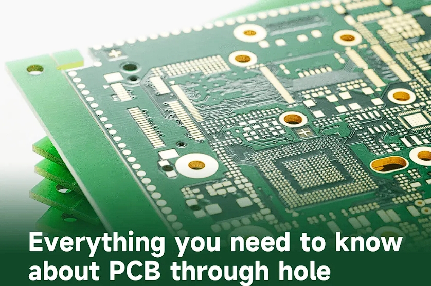
Through-hole PCB assembly involves the insertion of electronic components into pre-drilled holes on a PCB. These components are then soldered onto the board from the opposite side, forming a secure electrical connection. This technique offers several advantages, including increased mechanical strength, durability, and the ability to handle higher currents and voltages compared to surface-mount technology (SMT).
The process begins with the fabrication of the PCB, where a design layout is created and transferred onto a substrate material such as fiberglass-reinforced epoxy laminate. Pre-drilled holes are then strategically placed according to the circuit design. Once the PCB is ready, electronic components such as resistors, capacitors, diodes, and integrated circuits are selected and prepared for assembly.
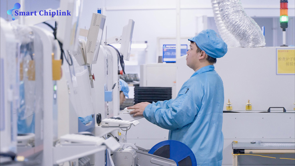
During assembly, technicians carefully place each component into its corresponding hole on the PCB. This step requires precision and attention to detail to ensure proper alignment and fit. Once all components are in place, the PCB undergoes a soldering process to create electrical connections. Traditional through-hole soldering methods include wave soldering and hand soldering.
Wave soldering involves passing the PCB over a wave of molten solder, which flows through the holes and forms solder joints with the component leads. This method is efficient for mass production but may require additional steps to protect sensitive components from heat damage. Hand soldering, on the other hand, offers more control and flexibility, allowing technicians to solder individual components manually using a soldering iron.
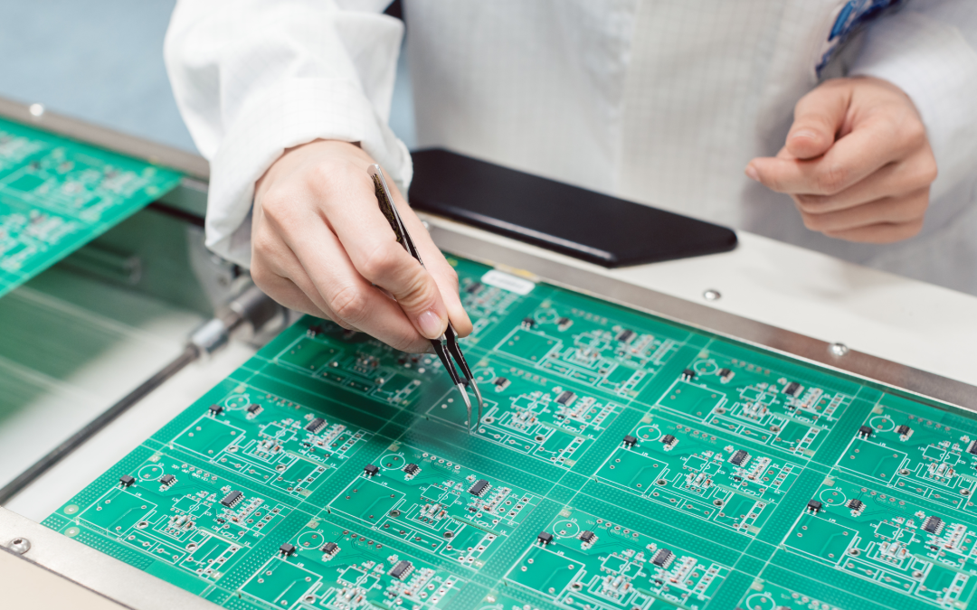
After soldering, the PCB undergoes inspection to detect any defects or soldering irregularities. Automated optical inspection (AOI) and X-ray inspection are commonly used to identify issues such as solder bridges, cold joints, or missing components. Once inspected and tested, the PCB is ready for further processing or integration into electronic devices.
Through-hole PCB assembly remains a fundamental technique in the electronics industry, particularly for applications where reliability, robustness, and ease of repair are paramount. While surface-mount technology continues to dominate modern electronics manufacturing, through-hole assembly continues to play a vital role in various industries, including aerospace, automotive, and industrial electronics.
As technology advances and new manufacturing processes emerge, the through-hole PCB assembly process continues to evolve, ensuring that electronic devices meet the demands of today's interconnected world.
 English