Why use Xilinx FPGA XC3S500E-4FTG256I?
If you are electronics engineering designer, you may know the XC3S500E-4FTG256I chip.
This Field Programmable Gate Array (FPGA) is widely used in various applications, from consumer electronics to Industrial control, aviation, military and other fields.
An FPGA is a semiconductor device consisting of a matrix of Configurable Logic Blocks (CLBs) connected through programmable interconnects. The user determines these interconnections by programming SRAM. A CLB can be simple (AND, OR gates, etc) or complex (a block of RAM). The FPGA allows changes to be made to a design even after the device is soldered into a PCB.
In this article, you will learn about some basics of the XC3S500E-4FTG256I of Xilinx, and also explore the professional way to use it and its features.
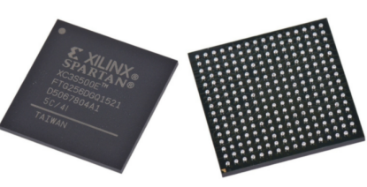
What Is XC3S500E-4FTG256I?
XC3S500E-4FTG256I belongs to Spartan-3E FPGA series, designed by Xilinx.
The Spartan-3E family offers a cost-effective FPGA solution with low power consumption, high performance, and advanced system-level features.
Xilinx Zynq FPGA
XC3S500E-4FTG256I features 500,000 system gates, 772 user I/Os, and 36 block RAMs.
It operates at a maximum frequency of 400MHz and has a core voltage range of 1.14V to 1.26V.
XC3S500E-4FTG256I is commonly used in applications, such as aerospace and defense, automotive, broadcast, consumer, high-performance computing, industrial, medical, and scientific, test, and measurement.
Request Original & New Xilinx XC3S500E-4FTG256I FGPA Now
Features of XC3S500E-4FTG256I
• SelectIO signaling
- Up to 633 I/O pins
- Eighteen single-ended signal standards
- Eight differential signal standards including LVDS and RSDS
- Double Data Rate (DDR) support
• Logic resources
- Abundant logic cells with shift register capability
- Wide multiplexers
- Fast look-ahead carry logic
- Dedicated 18 x 18 multipliers
- JTAG logic compatible with IEEE 1149.1/1532
• SelectRAM hierarchical memory
- Up to 1,728 Kbits of total block RAM
- Up to 432 Kbits of total distributed RAM
• Digital Clock Manager (four DCMs)
- Clock skew elimination
- Frequency synthesis
- High-resolution phase shifting
 English