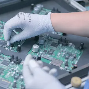
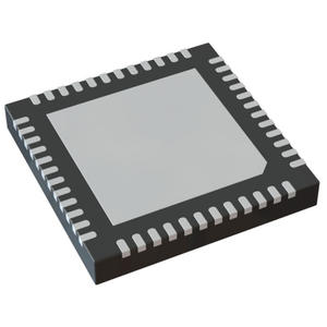
4 Layer electronic FR4 Printed Circuit Board Assembly
1.6mm 2OZ 4 Layer electronic FR4 Printed Circuit Board Assembly
Detailed Product Description
|
SMT And DIP:
|
Support
|
Application:
|
Camera PCBA
|
|
Components:
|
Supplied By Customers Or Supplied By Manufacturer
|
PCB Test:
|
AOI ; 100%test For Open And Short;
|
|
PCBA Test:
|
X-ray,Function Test
|
PCB:
|
HDI With Laser And Buried Holes
|
|
Soldermask:
|
Green/Bule/Black/white
|
Material:
|
FR4
|
|
Layer:
|
4 Layers
|
Copper:
|
2 OZ
|
|
High Light:
|
1.6mm 4 Layer PCB Manufacturer,
Camera FR4 Printed Circuit Board,
4 Layers FR4 Printed Circuit Board
|
1. Description Of PCB Assembly Service
this board is 4 layer it is used for Camera PCB . we can accept PCBA prototype,samll volum, middle and large volume. no MOQ request for new order.all of our PCB are met UL, TS 16949,ROHS, ISO etc. certification.
2. Specification Of PCB Assembly Service
|
Number of layers:
|
Mulity Layer / 4 layer
|
Surface finishing:
|
Gold Flash
|
|
Base material:
|
FR4
|
Solder mask:
|
LPI
|
|
Copper thickness:
|
2 oz Cu in all layer
|
Solder mask:
|
Green
|
|
Thickness:
|
1.66 mm
|
Working panel size :
|
max:1200mmX600mm (47'' X24'')
|
|
Size:
|
150.6 x 200.5 mm
|
Outline profile:
|
Punching, Routing , CNC routing + V-cut
|
|
Cooper In holes:
|
min 20um
|
Certificate :
|
UL, CQC, TS16949, ISO14000, ROHS
|
|
Solder mask :
|
LPI Solder mask, Peelable mask
|
Twist and Bow :
|
no more than 0.75 %
|
3. AutomotiveProducts Application:
1, Telecom Communication
2, Consumer Electronics
3, Security monitor
4, Vehicle Electronices
5, Smart Home
6, Industrial controls
7, Military & Defense
8, Smart Home
9, Industrial Automation
10, Medical Devices
11, New Energy
And so on
4. OEM/ODM/EMS Services For PCBA:
· PCBA, PCB Board assembly: SMT & PTH & BGA
· PCBA and enclosure design
· Components sourcing and purchasing
· Quick prototyping
· Plastic injection molding
· Metal sheet stamping
· Final assembly
· Test: AOI, In-Circuit Test (ICT), Functional Test (FCT)
· Custom clearance for material importing and product exporting
5. FAQ
Q: What files do you use in PCB fabrication?
A: Gerber or Eagle, BOM listing, PNP and Components Position
Q:Is it possible you could offer sample?
A: Yes, we can custom you sample to test before mass production
Q: When will I get the quotation after sent Gerber, BOM and test procedure?
A: Within 6 hours for PCB quotation and around 24-48 hours for PCBA quotation.
Q: How can I know the process of my PCB production?
A: 5-7days for PCB production and components purchasing, and 14 days for PCB assembly and Testing.
Q: How can I make sure the quality of my PCB?
A: We ensure that each piece of PCB products work well before shipping. We'll test all of them according to your test procedure.
 English
